Category: Lighting

  • Shuji Nakamura on 2nd and 3rd Generation Solid State Lighting

    Shuji Nakamura on 2nd and 3rd Generation Solid State Lighting

    Shuji Nakamura’s invention to save energy corresponding to about 60 nuclear power stations by 2020

    2nd and 3rd Generation Solid State Lighting

    For Shuji Nakamura’s invention of high-efficiency GaN double-heterostructure LEDs he was awarded the Nobel Prize in Physics 2014, while his employer sued him in the USA for leaking intellectual property – Shuji Nakamura won this court case, and his employer lost the case. To defend himself and his family, Shuji Nakamura countersued in Japan, and the Japanese court awarded Shuji a substantial award in a settlement. Shuji shared some insights into the comparison of IP lawsuits in US vs Japan with us at the 8th Ludwig Boltzmann Forum.

    Shuji moved to the University of California Santa Barbara, and is now building the company Soraa in Silicon Valley with investments from major US VC funds. Soraa may already be or is likely to be soon much bigger in value than Shuji’s previous Japanese employer. Soraa develops 2nd and 3rd Generation Solid State Lighting products.

    Energy savings corresponding to 60 nuclear power stations by 2020

    The global lighting revolution triggered by Shuji Nakamura’s inventions leads to energy savings corresponding to 60 nuclear power stations by 2020 – 60 nuclear power stations less will need to be built than without Shuji Nakamura’s inventions.

    2nd Generation and 3rd Generation Solid State Lighting

    With his venture company Soraa, Shuji is now working on 2nd Generation Solid State Lighting (GaN on GaN substrates) and 3rd Generation Solid State Lighting (laser lighting, which allows much higher light density), and which is already in use for car headlights.

    Why squeeze Nobel Prize winner Shuji Nakamura into a top-down narrative?

    Shuji Nakamura showed with a long list of newspaper clippings, TV show extracts, and Japanese Government agency announcements that he is being squeezed into a top-down innovation narrative, which is at odds with the findings of the Nobel Prize Committee of the Swedish Academy of Science.

    Shuji Nakamura asks why he is being squeezed retrospectively into a top-down innovation narrative.

    The truth is that most real innovation is bottom-up and disruptive, not government planned and top-down.

    At the 8th Ludwig Boltzmann Forum we had intense discussions between Her Imperial Highness, Princess Takamado, Professor Makoto Suematsu, Nobel Prize Winner Shuji Nakamura, Professor Nomura, JST-President Michinari Hamaguchi, and several other Japanese technology and R&D leaders.

    Read a summary of Shuji Nakamura’s talk here.

    Copyright (c) 2016 Eurotechnology Japan KK All Rights Reserved

  • Japan in 2015 – analysis

    Japan in 2015 – analysis

    Thoughts and analysis for 2015

    Abenomics?!

    The trick of course is the third arrow, the reforms. Read what Professor Takeo Hoshi has to say about Abenomics, Japanese economist, who has worked his way up US Universities, and has now reached the position of Professor of Economics at Stanford University. By the way, here is my talk at Stanford University – some years ago, but much of it still applies today.

    Japan’s energy

    Japanese people’s views on nuclear power are polarized, and its unclear and unpredictable when nuclear power stations will be switched on again in Japan. Read what the Governor of Niigata Prefecture has to say, who hosts the world’s largest nuclear power plant with 7 reactors and 8 GigaWatt capacity.

    According to the Japanese Energy Fundamental Law, the Government has to publish an official Energy Basic Plan at regular intervals. You can read the 4th Energy Basic Plan published on April 11, 2014, and listen to a commentary on it for The Economist here on YouTube. The 4th Energy Basic Plan starts with the assumption that Japan is poor in natural energy resources, which of course is only true if we restrict “natural energy resources” to fossil resources. Japan is actually potentially very very rich in renewable energy sources, as the scenario plans developed by Japan’s Industry and Economy Ministry (METI) and Japan’s Environmental Ministry show.

    Solid state lighting saves energy

    GaN LEDs were invented and commercialized in Japan, and Shuji Nakamura, Isamu Akasaki and Hiroshi Amano won the 2014 Nobel Prize in Physics for this work. Read the summary of Shuji Nakamura’s keynote at the 5th Ludwig Boltzmann Forum.

    Post-Galapagos and globalization of Japan’s technology groups

    To overcome Japan’s Galapagos issues and to acquire technologies and market access, Japanese companies are acquiring overseas: read a list of Japanese acquisitions in Europe here.

    Foreign companies in Japan, and Japanese companies overseas face a dilemma: expensive expatriates with limited local know-how, or local management? Japanese companies seem to have finally reached the conclusion that Japanese managers eg sent to Germany are in most cases not the best choice to lead a German-based multinational company – here are some great recent examples:

    • Docomo acquires a majority stake in net mobile AG, however net mobile AG remains a publicly listed company. Read details here.
    • NTT DATA acquires SAP solution provider itelligence AG, however itelligence AG remains an independently managed company under the founder’s management, and grows aggressively via acquisitions all over the globe. Read details here.
    • NTT Communications acquires a majority of Integralis, Integralis is renamed NTT Com Security AG, however NTT Com Security AG remains traded on the m:access market of the Munich Stock Exchange. Read details here.

    Carlos Ghosn is very well aware of such multi-cultural management issues and how to solve them, however too many EU companies in Japan are not. If they were, EU investments in Japan could be at least 50% higheras you can read here.

    Best wishes, and much success in 2015!

    Copyright 2015 Eurotechnology Japan KK All Rights Reserved

  • Shuji Nakamura: did he invent the blue GaN LED alone and other questions. An Interview.

    Shuji Nakamura: did he invent the blue GaN LED alone and other questions. An Interview.

    Interview for the Chinese Newspaper Southern Weekly about Shuji Nakamura
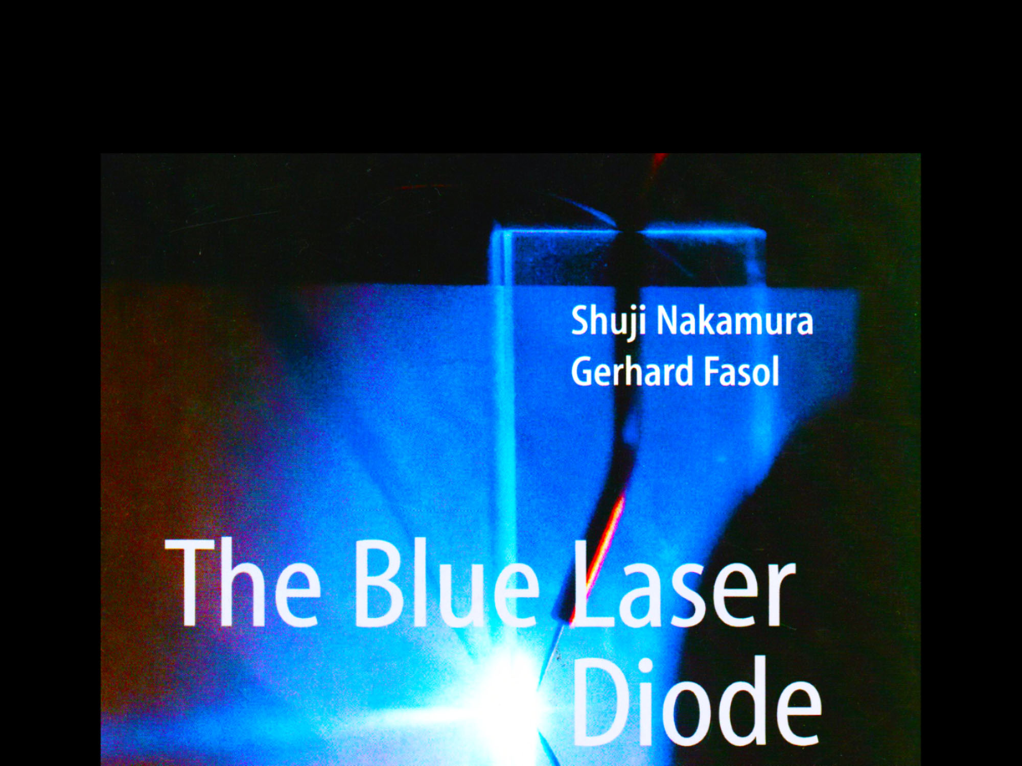
    by Gerhard Fasol

    The Chinese Newspaper Southern Weekly interviewed me about Shuji Nakamura’s invention of the blue LED and the background to his Nobel Prize. Here some of my answers.

    Read the article in Southern Weekly in Chinese language here: 【2014诺贝尔·科学】无人相信的发明

    Shuji Nakamura: when he first announced his breakthrough, most people just did not believe him initially. But you are an exception. What made you believe in Dr Nakamura?

    At the time when I first heard Shuji Nakamura’s results around 1992 – long before Bob Johnstone hear about these results (Bob Johnston is a friend of mine, and I know him for a long time – but Bob Johnstone is a journalist, I am a Physicist) I had worked about 18 years in physics research, at many of the best research labs in the world. So I had at that time already a very long experience in research. When I heard Shuji Nakamura’s talk at the Physics Conference in Nagoya, I could immediately judge from his talk that this was a very very important result. So I visited Shuji Nakamura at his laboratory at the company Nichia in Anan several times for discussions, he gave me copies of his papers and patents and I studied his research papers and his patents, and he also showed me the blue LEDs so I could see for myself. I had worked a long time in this field already, so I could understand that his work was true, and I could also see the working blue LEDs with my own eyes. Such blue LEDs did not exist before, so it was clear that he had succeeded in this breakthrough.

    At that time I knew almost all research groups in the world working on blue LEDs, at IBM, Hitachi, SONY, and many University labs and national labs globally, and I knew the status of their research. It was obvious that Shuji Nakamura had won this race.

    It is true that many people did not believe his results initially. That was because these people did not make the same effort that I made to visit Shuji Nakamura and study his results.

    For example, I send a report about Shuji Nakamura’s breakthrough to the German Physical Society member’s journal for publication, and the Editor rejected my article initially, because he showed this report to German Professors in this field. They had not heard about Shuji Nakamura’s work, so they had never heard about this blue LED breakthrough and were working in their own labs on II-VI compounds which was a dead end. Because they considered themselves as the top experts in the field they rejected my report on Shuji Nakamura’s work.

    I told the Editor that I am right, and the German experts are wrong, the Editor believed me and printed my report about Shuji Nakamura’s work. You can read this report online here (in German language):
    http://onlinelibrary.wiley.com/doi/10.1002/phbl.19950511004/abstract

    Some researchers question whether Dr Nakamura made the blue LED on his own. Why do people criticise his achievement and what is the truth? Do these rumors continue after the Nobel Prize was announced?

    Every researcher “stands on the shoulder of giants”, of course now work is done in total isolation, and always rests on some previous results. Even Einstein, who did not read many scientific papers and worked out many results on his own from zero point, of course used many results of others.

    Therefore Shuji Nakamura’s work of course relied on the hard work of many other researchers before him. For example he used the production technology called MOCVD (Metal Organic Chemical Vapor Deposition), which he learned in Professor Ramaswamy’s group at the University of Florida (Professor Ramaswamy was working in the office next to mine at Tokyo University for about 1 year, so I know him also very well). Shuji Nakamura also could read the published part of Professor Akasaki and Professor Amano’s excellent results on GaN compounds – Professor Akasaki and Amano’s work were also awarded the Nobel Prize at the same time as Shuji Nakamura.

    Shuji Nakamura could not have done his work without the support of the Founder and Chairman at that time of the company Nichia, Mr. Nobuo Ogawa. Shuji Nakamura introduced me to his Chairman Mr Nobuo Ogawa and I had lunch with him several times and discussed how he supported Shuji Nakamura’s work financially and as the leader of Nichia. Mr Nobuo Ogawa at that time owned about 1/3 of the company Nichia, so he could take major decisions such as supporting Shuji Nakamura.

    I believe that at Nichia there are two people without whom this work would not have happened:

    1. Chairman Nobuo Ogawa and
    2. Shuji Nakamura

    Neither could have done the work alone, and both together were necessary to achieve this
    breakthrough at Nichia. Also, when Shuji Nakamura went to Mr Nobuo Ogawa and proposed to work towards the discovery of blue GaN LEDs, at that time, Shuji Nakamura did not have a PhD, and no great research success stories behind him, although he has done successful development of red LEDs, but which were not commercially successful. Without a PhD I think there would have been almost no one except Mr Nobuo Ogawa who would have supported Shuji Nakamura’s proposal, certainly no large corporation, government supported research agency, or University, and without a PhD he would have had zero chance to win a peer-reviewed research grant from large research agencies.

    Unfortunately Mr Nobuo Ogawa passed away some years ago, so he cannot enjoy the Nobel Prize celebrations.

    Of course at Nichia, Shuji Nakamura could attract a number of very excellent assistant researchers, but it is very clear that Shuji Nakamura was the leader of the Blue LED research at Nichia who was leading a group of assistant researchers who essentially followed his leadership and were doing this work because of him and under Shuji Nakamura’s leadership. I am very convinced that if Shuji Nakamura would not have been working at Nichia, this invention would not have happened at Nichia. This is quite obvious to anyone who understands how science works.

    Of course there are some people who envy Shuji Nakamura. Excellent people celebrate Shuji Nakamura’s success and get inspired. Mediocre people spend their time spreading rumors and talking bad about Shuji Nakamura, don’t listen to them. I have heard some of these rumors, and I have checked most of them direct with Shuji Nakamura, and I am convinced that these rumors are wrong.

    Maybe some of the people who spread stupid rumors about Shuji Nakamura have failed in their own work, and don’t like someone else succeed?

    About the Nobel Prize: The Nobel Prize in Physics is decided by the Nobel Prize in Physics Committee of the Swedish National Academy of Science. When I have worked in Europe, I met some of the members of this committee and I can tell you that they are all very very excellent Physicist. I am convinced that they are doing a very excellent job in checking in great detail how Shuji Nakamura achieved his results, and I am sure they have checked out all these rumors and found that they are untrue.

    As a colleague of Dr Nakamura’s, could you describe a little bit about his style in research?

    First of all like all excellent researchers Shuji Nakamura is extremely passionate, driven by passion for his work, and he is a maniac, working very very hard. When I was working on the book with Shuji, he was working with me on 30., 31., December, 1st of January all over the New Year period without break, exchanging emails with me in the middle of the night etc.

    Secondly he is driven by intuition – he is a genius. Maybe you know that when Shuji studied at the University of Tokushima, the University did not have a Physics Department, so Shuji did not study full Physics but won the Physics Nobel Prize! I am Physicist, I have full Physics University training even to a PhD level, and I can tell you that Shuji has a very deep understanding of Physics, but he has essentially learnt this all by himself! Not through a University Physics degree!

    I think his work is very intuitive. He has a very deep understanding of Nature, and follows his intuitions, his feelings, much more than anything he has learnt from the books.

    More information:

    Copyright 2014-2019 Eurotechnology Japan KK All Rights Reserved

  • Shuji Nakamura, Isamu Akasaki, Hiroshi Amano win Nobel Prize in Physics 2014 for the blue LED

    Shuji Nakamura, Isamu Akasaki, Hiroshi Amano win Nobel Prize in Physics 2014 for the blue LED

    Nobel Prize in Physics 2014 for the blue GaN LED

    by Gerhard Fasol

    Shuji Nakamura, Isamu Akasaki, Hiroshi Amano enabled the global lighting revolution

    The Nobel Prize in Physics 2014 was awarded in equal shares to Isamu Akasaki, Hiroshi Amano and Shuji Nakamura “for the invention of efficient blue light-emitting diodes which has enabled bright and energy-saving white light sources”.

    While red and green LEDs were invented long ago, efficient blue LEDs did not exist until Akasaki’s, Amano’s and Nakamura’s long series of inventions. Blue LEDs are needed to create white light.

    The invention of blue GaN based LEDs enables the global lighting revolution. By replacing legacy light bulbs, fluorescent tubes etc by GaN LEDs, a big fraction of the world’s electricity can be saved, and the effect is even bigger in the developing world where still today many people use extremely expensive oil for lighting. Read a detailed analysis of the economics of lighting here.

    The mainstream blue-LED scientific community was working on a dead-end: II-VI compounds

    Of course the importance of blue LEDs was understood for a long time, and in the 1980s and 1990s all major industrial and University labs were working towards this holy grail – Hitachi, SONY, Philips, IBM, lots of Universities in Europe and US and elsewhere had groups working towards blue LEDs – but they all worked on II-VI compounds, which turned out to be a dead end.

    The way much (not all – and thats the way towards Nobel Prize class discoveries) of mainstream established incremental research works, in most established labs, to get peer reviewed grants for research towards blue LEDs in the 1980s, this had to be II-VI work.

    It needed strong willed people as Shuji, Akasaki and Amano to take a totally different approach outside the mainstream. Its to the credit of JST and other Japanese funding agencies to have supported Amano and Akasaki’s work. Shuji on the other hand ‘only’ had one person to convince: the owner and founder of Nichia Mr Nobuo Ogawa- and did I say that Shuji did not have a PhD at that time?

    Which research agency would give a couple of million $ to a researcher without a PhD but with a big almost unreachable target who still has to learn the methods (MOCVD in this case) to work towards this target – other than Mr Nobuo Ogawa?

    Shuji Nakamura actually introduced me to Mr Nobuo Ogawa in Anan (Tokushima-ken), and we had several curry lunches in a restaurant next to Nichia Chemical Industries Headquarters. I asked Nichia-Chairman and Founder Nobuo Ogawa how he decided at the time to fund Shuji Nakamura’s one-year stay at the University of Florida in Professor Ramaswamy’s group to learn MOCVD (by the way Professor Ramaswamy was my office-neighbour when I was Associate Professor on the NTT Telecommunications Chair at Tokyo University), and fund Shuji Nakamura’s work to the tune of many US$ million, which at that time was a large fraction of Nichia’s overall sales.

    To my question how Mr Nobuo Ogawa took the decision to support Shuji Nakamura, Mr Nobuo Ogawa simply answered: “How did you chose your wife, Gerhard?”.

    Shuji Nakamura, Isamu Akasaki, Hiroshi Amano worked on III-V compounds and achieved the lighting breakthrough

    While the mainstream scientific blue-LED community worked with high intensity towards this dead end without knowing that they devoted their lives and their students to a dead-end, Akasaki and Amano over many years painstakingly solved one problem after another to create electronic devices based on the III-V compound semiconductor GaN and its variations.

    Shuji Nakamura then built on Akasaki and Amano’s work, solved the three major and many many minor problems remaining to create commercially viable blue LEDs. But the work did not stop there: Shuji Nakamura also created white LEDs, UV LEDs, blue Lasers (e.g. for SONY’s blue-ray DVD players and displays) and a lot more. (read about Shuji Nakamura’s breakthrough work in great technical detail here: The Blue Laser Diode)

    Shuji Nakamura, Nichia Kagaku Kougiyou and releasing Japan’s creative power

    Shuji Nakamura was also a very diligent writer of patents and wrote a large number of very strong patents. These inventions together with patents propelled his then employer Nichia Kagaku Kougiou from a maker of phosphors (which were used for cathode ray tubes and fluorescent tubes) to one of the most important semiconductor companies. For these inventions, Nichia paid Shuji Nakamura a salary approximately on the level of a Japanese primary school teacher, plus a few US$ 100 bonus for the inventions.

    Lets not go into the law suits between Nichia and Shuji Nakamura here, but let me say, that I have never found the complete story explained in the media. Most media reports give a very incomplete picture of the true story of the law suits between Nichia and Shuji Nakamura. – I guess most media just copy from each other in this case…

    I noticed Shuji Nakamura’s work first around 1992 at the Japanese Applied Physics Conference in Nagoya, where Shuji gave a talk about his GaN work. I visited Shuji a couple of times in Anan (Tokushima-ken), he introduced me to the founder of Nichia, Mr Nobuo Ogawa, without who’s support Shuji’s work would have been impossible. With Nobuo Ogawa’s death, Shuji decided to move to the USA, to Santa Barbara, where he is working today. Interestingly, when Shuji was looking for a job, he had lots of offers from USA, but none from Europe and none from Japan… Why that?

    Shuji developed deep insights about issues holding back Japan, and has shared his advice on many occasions, including also the Ludwig Boltzmann Forum, which I annually organize in Tokyo as a leadership platform. Read about his talk here, where Shuji passionately calls for changes – even a revolution – in Japan, to unshackle Japan’s creative energies.

    To learn more about the Blue GaN LEDs and lasers, and their invention:

    and of course you can also read Shuji Nakamura’s, Isamu Akasaki’s and Hiroshi Amano’s 100s or even 1000s of original scientific publications.

    Shuji Nakamura talking passionately at the Ludwig Boltzmann Forum in Tokyo 2013
    Shuji Nakamura talking passionately at the Ludwig Boltzmann Forum in Tokyo 2013

    Copyright (c) 2014 Eurotechnology Japan KK All Rights Reserved

  • VCSEL – Vertical cavity surface emitting lasers by their inventor, Kenichi Iga (6th Ludwig Boltzmann Symposium)

    VCSEL – Vertical cavity surface emitting lasers by their inventor, Kenichi Iga (6th Ludwig Boltzmann Symposium)

    VCSEL inventor Kenichi Iga: hv vs kT – Optoelectronics and Energy

    (Former President and Emeritus Professor of Tokyo Institute of Technology. Inventor of VCSEL (vertical cavity surface emitting lasers), widely used in photonics systems)

    Keynote presented at the 6th Ludwig Boltzmann Symposium on February 20, 2014 at the Embassy of Austria in Tokyo.

    VCSEL: how Kenichi Iga invented Vertical Cavity Surface Emitting Lasers

    My invention of vertical cavity surface emitting lasers (VCSEL) dates back to March 22, 1977. Today VCSEL devices are used in many applications all over the world. I was awarded the 2013 Franklin Institute Award, the Bower Award and Prize for Achievement in Science, “for the conception and development of the vertical cavity surface emitting laser and its multiple applications in optoelectronics“. Benjamin Franklin’s work is linked to mine: Benjamin Franklin in 1752 discovered that thunder originates from electricity – he linked electronics (electricity) with photons (light). After 1960 the era of lasers began, we learnt how to combine and control electrons and photons, and the era of optoelectronics.

    If you read Japanese, you may be interested to read an interview with Genichi Hatakoshi and myself, intitled “The treasure micro box of optoelectronics” which was recently published in the Japanese journal OplusE Magazine by Adcom-Media.

    Electrons and photons

    Who are electrons? Electrons are just like a cloud expressed by Schroedinger’s equation, which Schroedinger postulated in 1926. Electrons can also be seen as randomly moving particles, described by the particle version of Schroedinger’s equation (1931).

    Where does light come from? Light is generated by the accelerated motion of charged particles.

    Electrons also show interference patterns. For example, if we combine the 1s and 2p orbitals around a nucleus, we observe interference.

    In a semiconductor, electrons are characterized by a band structure, filled valence bands and largely empty conduction bands. The population of hole states in the valence bands and of electrons in the conduction bands are determined by the Fermi-Dirac distribution. In typical III-V semiconductors, generation and absorption of light is by transitions between 4s anti-bonding orbitals (the bottom of the conduction band) and 4p bonding orbitals (the top of the valence band).

    In Japan, we are good at inventing new types of vertical structures:

    • in 607, the Horyuji 5-Jyu-no Toh (5 story tower) was built in Nara, and today we have progressed to building the 634 meter high Tokyo Sky Tree Tower.
    • in 1893, Kubota Co. Ltd. developed the vertical molding of water pipes
    • in 1977 Shunichi Iwawaki invented vertical magnetic memory
    • in 1977 Tatsuo Izawa developed VAD (vapor-phase axial deposition) of silica fibers
    • in 1977 Kenichi Iga invented vertical cavity surface emitting lasers (VCSEL)

    Communications and optical signal transmission

    History of communications spans from 10,000 years BC with the invention of language, and 3000 BC with the invention of written characters and papyrus, to the invention of the internet in 1957, the realization of the laser in 1960, the realization of optical fiber communications in 1984, and now since 2008 we see Web 2.x and Cloud.

    Optical telegraphy goes back to 200 BC, when optical beacons were used in China: digital signals using multi-color smoke. Around 600 AD we had optical beacons in China, Korea and Japan, and in 1200 BC also in Mongolia and India.
    In the 18th and 19th century, optical semaphores were used in France.

    In the 20th century, optical beam transmission using optical rods and optical fiber transmissions were developed, which combined with the development of lasers created today’s laser communications. Yasuharu Suematsu and his student showed the world’s first demonstration of optical fiber communications demonstration on May 26, 1963 at the Tokyo Institute of Technology, using a He-Ne laser, an electro-optic crystal for modulation of the laser light by the electrical signal from a microphone, and optical bundle fiber, and a photo-tube at the other end of the optical fiber bundle to revert the optical signals back into electrical signals and finally to drive a loud speaker. For his pioneering work, Yasuharu Suematsu was awarded the International Japan Prize in 2014.

    VCSEL: I recorded my initial idea for the surface emitting laser on March 22, 1977 in my lab book.

    Vertical Cavity Surface Emitting Lasers (VCSEL) have many advantages:

    1. ultra-low power consumption: small volume
    2. pure spectrum operation: short cavity
    3. continuous spectrum tuning: single resonance
    4. high speed modulation: wide response range
    5. easy coupling to optical fibers: circular mode
    6. monolithic fabrication like LSI
    7. wafer level probe testing
    8. 2-dimensional array
    9. vertical stack integration with micro-machine
    10. physically small

    VCSEL have found applications in many fields, including: data communications, sensing, printing, interconnects, displays.

    As an example, the Tsubame-2 supercomputer, which in November 2011 was 5th of top-500 supercomputers, and on June 2, 2011 was greenest computer of Green500, uses 3500 optical fiber interconnects with a length of 100km. In 2012: Too500/Green500/Graph500

    IBM Sequoia uses 330,000 VCSELs.

    Fuji Xerox introduced the first demonstration of 2 dimensional 4×8 VCSEL printer array for high speed and ultra-fine resolution laser printing: 14 pages/minute and 2400 dots/inch.

    VCSEL: Some recent news:

    The laser market is estimated to be US$ 11 billion by 2017.
    VCSELs move to optical interconnects.
    By 2019 the optical interconnect market is estimated to reach US$ 5.2 billion.

    VCSEL: In summary

    VCSEL photonics started from minor reputation and generated big innovation. VCSELs feature:

    • low power consumption: good for green ICE
    • high speed modulation beyond 20 GBits/second
    • 2D array
    • good productivity due to monolithic process

    Future: will generate ideas never thought before.

    VCSEL em. President of Tokyo Institute of Technology, Professor Kenichi Iga, inventor of VCSEL
    em. President of Tokyo Institute of Technology, Professor Kenichi Iga, inventor of VCSEL
    VCSEL Gerhard Fasol (left), em. President of Tokyo Institute of Technology, Professor Kenichi Iga (right)
    Gerhard Fasol (left), em. President of Tokyo Institute of Technology, Professor Kenichi Iga (right)

    Copyright (c) 2014 Eurotechnology Japan KK All Rights Reserved

  • Blue laser book with Shuji Nakamura – how this book came about

    Blue laser book with Shuji Nakamura – how this book came about

    The Blue Laser Diode, by Shuji Nakamura and Gerhard Fasol, Springer Verlag

    The story and physics background of the discovery and development of the GaN LEDs and lasers

    Since I have been working for many years on GaAs research, as soon as I heard Shuji Nakamura’s talk at one of Japan’s applied physics conferences, I understood the importance, visited Shuji Nakamura in Anan where he was working at Nichia Kagaku Kougiyou, and became friends with Shuji Nakamura. Shuji Nakamura also introduced me over curry lunch to Founder and Chairman Nobuo Ogawa (小川 信雄), who at that time was about 83 years old.

    I asked Chairman Nobuo Ogawa why he had agreed to pay for Shuji Nakamura’s proposed research on GaN blue LEDs, and pay for Shuji Nakamura learn MOCVD at the University of Florida in Professor Ramaswamy’s group. Nobuo Ogawa’s answer: “How did you chose your wife?”

    I wrote a number of articles about Shuji Nakamura’s development of GaN LEDs and lasers in SCIENCE Magazine and the Deutsche Physikalische Blätter.

    “Physikalische Blätter” initially rejected the first report on GaN LEDs – German experts had never heard about this discovery before, therefore rejected it as incredible

    I also wrote an article for the Journal of the German Physical Society, at that time “Physikalische Blätter”, for which I was regularly writing articles and reports from Japan. The Editor initially rejected my article. He told me that he had consulted with German experts, and these experts had told him that they had never heard about a successful blue GaN LED, and that this was therefore impossible, and wrong. The Editor asked me rhetorically: “Do you think these German experts are wrong?” – I answered “Yes, they are wrong – you should publish this article”, and sent him some background information in support of my article. He finally published the article, and you can find it online here:

    • Gerhard Fasol: “Die blaue GaN Leuchtdiode: Auftakt für einen neuen Industriezweig (The blue GaN light emitting diode: the beginning of a new industry)” Physikalische Blätter, 51, p. 925-926 (October 1995)
    • Gerhard Fasol: “Japanische Herbstkonferenzen in Angewandter Physics (Japan’s autumn conferences on applied physics)” Physikalische Blätter, 50, p. 1118-1119 (December 1994) (my first report on Shuji Nakamura’s GaN work in Germany’s Physikalische Blätter)

    Through my articles in Science Magazine and Physikalische Blätter, Claus Ascheron, Physics Editor of Springer Verlag became aware of my work in Tokyo, and asked me if I can help him win Shuji Nakamura’s agreement to write a book on his GaN work.

    Blue laser book – how it came about

    Claus Ascheron and myself went to visit Shuji Nakamura, and we had a lunch with Shuji Nakamura, Chairman Nobuo Ogawa, Claus Ascheron and myself. During lunch Claus Ascheron asked Shuji Nakamura, if he would be interested to write a book for Springer Verlag. Shuji agreed, but said that he needs Chairman Ogawa’s agreement. He asked Chairman Ogawa straight away, and Chairman Ogawa said “No. You can’t write this book, I don’t give my permission”. So I intervened and asked Chairman Ogawa for the reason of this refusal. Chairman Ogawa said: “Nakamura-san is researcher, he must do research and develop new products, he cannot waste his time writing books”. So I offered to help as a co-author, so that this would take less of Shuji Nakamura’s time. Chairman Ogawa agreed to this arrangement, and gave his permission.

    As a result, Shuji Nakamura and myself worked many night-sessions over Christmas and New Year 1996/1997, and the first edition of the Blue GaN Laser book was published in January 1997, to be ready for the annual Book Fair in Frankfurt.

    • “The Blue Laser Diode : The Complete Story” (2nd Edition),
      S. Nakamura, S. Pearton, G. Fasol
      (Springer-Verlag, October 2000, ISBN 3-540-66505-6)
      Press here to order “The blue laser diode” from amazon.com

    • “The Blue Laser Diode – GaN based light emitters and lasers” (1st Edition),
      S. Nakamura, G. Fasol
      (Springer-Verlag, January 1997, ISBN 987-3-662-03464-4)

    You can also read some of the background of Shuji Nakamura’s invention and the development of the solid state lighting industry in our Solid State Lighting report.

    Solid state lighting report:

    Copyright 2013 Eurotechnology Japan KK All Rights Reserved

  • Gallium Nitride LEDs for Christmas

    Gallium Nitride LEDs for Christmas

    Since Shuji Nakamura’s first commercialization of GaN LEDs (read the Blue Laser Diode Book) LEDs are progressing rapidly to make the US$ 400 Billion global lighting industry more environmentally friendly, reducing CO2 output and reducing electricity bills for lighting dramatically. Recently rail stations in Japan have begun to test plug-compatible replacement of fluorescent tubes by LED based solid state lighting.

    This year our company advised a number of investment fund managers on technology, business models, financial models and trends of the solid state lighting industry. Please find a detailed Solid State Lighting report here – we continuously update this report.

    Christmas lighting with blue LEDs in Tokyo Midtown. Tokyo Tower can be seen in the back, lighted using traditional lamps, though. Merry Christmas!

    Blue GaN LEDs in Tokyo/Midtown for Christmas illumination
    Blue GaN LEDs in Tokyo/Midtown for Christmas illumination

    Copyright (c) 2013 Eurotechnology Japan KK All Rights Reserved

  • Outsourcing Japan market research and strategy consulting to India, Philippines?? – a recipe for business failure in Japan?

    Outsourcing Japan market research and strategy consulting to India, Philippines?? – a recipe for business failure in Japan?

    Business decisions unrelated to market realities are a prime reason for failure of foreign companies in Japan

    In a quest to reduce market research costs, Japan market research is often outsourced to India, Philippines, Indonesia etc

    With shock and surprise we recently found out that a very famous telecom and IT industry market research and strategy consulting firm with a globally famous brand apparently outsources market research of Japan’s mobile phone and telecom sector to India. The Indian employees apparently are diligently studying the Japanese language in evening classes, so that in a few years time, they will be able to read a little of the Japanese mobile market information which can be found on the internet, we assume.

    We believe that this explains why so much information about Japan’s telecom and mobile phone markets circulating outside Japan is incomplete, or in many cases even wrong. As a consequence companies like Vodafone then take management decisions in Japan, which were totally unrelated to Japan’s market realities.

    This fact also contributes we believe to the fact, that some of the most famous global companies in the telecommunications sector find it so difficult to succeed in Japan – not that Vodafone, Nokia (mobile phones and VERTU – except networks which are a great success), Cable & Wireless, Deutsche Telekom all withdrew from Japan – outsourcing market intelligence to low-cost countries such as China, India, Philippines etc. is certainly one of the contributing factors.

    Indeed similar to Vodafone’s departure from Japan, famous global telecom consultancies have also closed shop in Japan, due to the very high costs and the continuous high investments necessary to achieve and maintain leadership in understanding Japan’s telecommunication markets.

    We can assure our newsletter subscribers and our customers that our original Eurotechnology market reports and our strategy consulting is hand crafted in Tokyo/Japan. Our team members working on Japan market research and strategy consulting, all live in Japan, are mostly Japanese, and work daily with Japanese CEOs, telecom managers, and most importantly of all, daily interview and discuss with real-life Japanese mobile phones users: face-to-face here in Japan – not across one or more oceans.

    Made in Japan: the Original “Eurotechnology” Japan-market reports

    Copyright (c) 2013 Eurotechnology Japan KK All Rights Reserved