Category: technology

  • Struggling for Europe’s technology sovereignty – a comment on Hermann Hauser’s proposal for a €100 billion Technology Sovereignty Fund

    Struggling for Europe’s technology sovereignty – a comment on Hermann Hauser’s proposal for a €100 billion Technology Sovereignty Fund

    by Gerhard Fasol

    Hermann Hauser in a recent article on Project Syndicate, entitled “The Struggle for Technology Sovereignty in Europe” argues for “the UK and EU to jointly establish a €100 billion ($120 billion) Technology Sovereignty Fund to counter the $100 billion that the US is spending on its technology sovereignty and the even larger amounts China is mobilizing”. I argue here, that we should be thinking that 27+1 countries could create much larger funds in a world where single individuals like Masayoshi Son can create funds of that order.

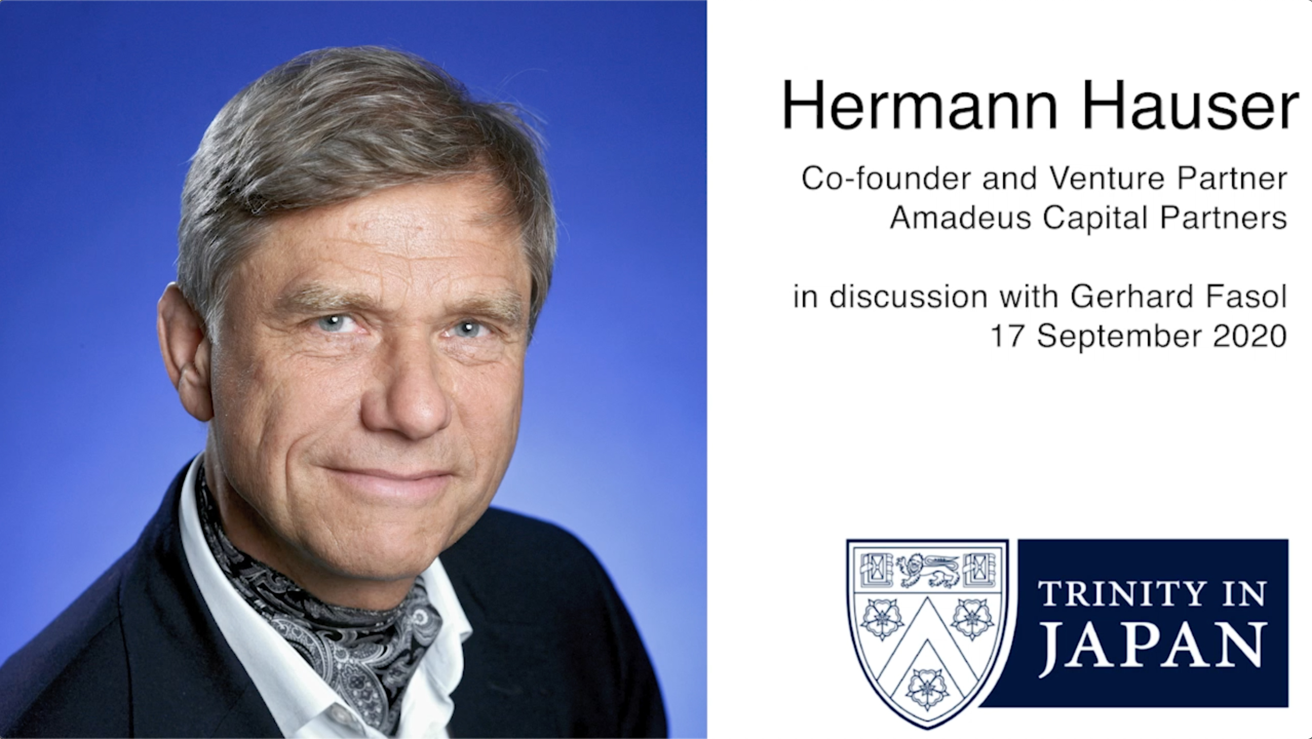
    Hermann Hauser became an entrepreneur right after finishing his PhD in the Cavendish Lab (Cambridge University, UK) around 1978 – on the same lab bench in the Cavendish as myself – and is arguably Europe’s first and most important technology venture investor. Hermann Hauser can be seen as the initiator of Europe’s VC industry. Hermann Hauser is also one of the co-founders of ARM and many other high-tech companies. For a discussion with Hermann see:

    The thought of a €100 billion Technology Sovereignty Fund is of course a fantastic plan. As a starting point, thats of course a great idea, however in my opinion, much much more is needed. My thought would be that for European Technology Sovereignty, five or ten, or even more funds of that €100 billion size will be needed. In my opinion, better not only by governments, but by private individuals like European versions of Masayoshi Son.

    Three thoughts, which I will illustrate below

    • a €100 billion fund for 27+1 countries is a lot smaller than the US$ 391 billion the single man Masayoshi Son is estimated to control (Vision funds plus three companies)
    • a €100 billion fund for 27+1 countries is much smaller than the sovereign funds of very much smaller countries:
      • Singapore (5.7 million people), sovereign funds: US$ 715 billion
      • Norway (5.3 million people), sovereign funds: US$ 1327 billion
    • My third point is that the assets in question (ARM) in Hermann Hauser’s Project Syndicate article would already use a large part of the proposed €100 billion fund.

    To put a €100 billion fund for 27 EU Countries + UK into context:

    Just one single man (Masayoshi Son, from a Korean immigrant family to Japan) controls at least two funds + and to some extent several companies, worth in total on the order of US$ 391 billion as follows:

    • the current “fair value” of the first + second Vision Funds is reported as US$ 154 Billion.
    • In addition, Masayoshi Son also controls (to some extent) the listed companies, which he often uses as acquisition and finance vehicles:
      • SoftBank Group Corp [TSE: 9984]: market cap = US$ 130 billion
      • SoftBank Corp [TSE: 9434]: market cap = US$ 67 billion
      • Z Holdings Corp [TSE:4689]: market cap = US$ 40 billion (includes Yahoo Japan Corp + LINE)

    That is just one single man, who created all this from zero, not 27+1 countries.

    Or as another comparison, Singapore has built at least two sovereign funds in total estimated to be worth US$ 715 billion. Singapore is one single relatively small country compared to 27+1 European countries (population of Singapore is about 5 million, about the same as Norway, and about the same as the Berlin region)

    1. Singapore Sovereign Wealth Fund GIC estimated value US$ 488 billion
    2. Temasec Holdings US$ 227 billion

    Norway’s sovereign funds (population about 5 million):

    1. Sovereign Pension Fund – Foreign US$ 1300 billion assets
    2. Sovereign Pension Fund – Norway US$ 27 billion assets

    My third point is that a single €100 billion fund is of comparable size of developed assets in question. eg. ARM’s current value would be a substantial part of a potential €100 billion fund. This means that after acquiring two or three companies of the value of ARM this fund would already be exhausted.

    As another example, the strategic German mRNA company BioNTech (which among other therapies developed the BioNTech Covid Vaccine in cooperation with Pfizer) has a current market cap of US$ 51 billion. If a situation would arise that such a Sovereign fund would acquire a company such as BioNTech, that would again use up a large fraction – if not almost all of this fund. In my opinion, although of course a €100 billion fund investing in European technology companies in addition to existing substantial VC and investment funds would be great, this is not huge – even relatively small – compared both to the value of many assets in question, and also to the funds some private individuals (eg Masayoshi Son) or 5 million people countries (like Singapore or Norway) manage to build.

    So I think many more than a single €100 billion fund would be needed for Technology Sovereignty – I hope circumstances will develop where even more can be invested in European ventures than today. Hermann Hauser’s proposal is certainly a great step in the right direction- many more such steps would be great!

    (c) 2021 Gerhard Fasol

  • International Nanotechnology Symposium in Tokyo 16 September 2019

    International Nanotechnology Symposium in Tokyo 16 September 2019

    21 University of Cambridge nanotechnology researchers in Tokyo

    日本語版

    Cambridge University nanotechnology researchers and PhD students
    Cambridge University nanotechnology researchers and PhD students

    日本語版

    International Nanotechnology Symposium in Tokyo

    21 University of Cambridge nanotechnology researchers in Tokyo meeting Japanese corporations

    Symposium chair and contact: Gerhard Fasol contact here

    Monday 16 September 2019 15:00-21:00 in Tokyo

    Purpose of the International Nanotechnology Symposium in Tokyo

    Exchange of views on results and future development of different nanotechnology fields between 21 Cambridge University nano-technology researchers and PhD students, researchers and nanotechnology companies. Explore common interests, and potential cooperation.

    University of Cambridge, founded 1209 AD

    • 107 Nobel Prize winners
    • around University of Cambridge: 4700 knowledge intensive companies, 560 high-tech manufacturing firms, 3000 IT and communication based companies
    • 2019 THE Times Higher Education Global University Ranking: Place 2 globally
    • 2019 ARWU Global University Ranking: Place 3 globally
    • 2019 QS Global University Ranking: Place 6 globally

    Program

    15:00 – 19:00

    • presentations by Cambridge nanotechnology researchers:
      • Session 1:  Nanotechnology for Energy & Sustainability
        • TU – Plastic waste as a feedstock for solar-driven hydrogen generation 
        • TL – Fibre-based optofluidics for sustainable photocatalysis
        • AG – Ultrafast charging Li-ion batteries
        • JM – Battery material degradation at the nanoscale studied by analytical electron microscopy
        • MJ – Understanding the nature of oxygen redox in Li-excess cation disordered rocksalts as cathode materials for Li-ion batteries
        • JT – Structure and ionic conductivity of metal-organic framework composites
        • TP – Light-induced patterning of structural colour
        • TB – Triboelectric textile for wearable energy harvesting
      •  Session 2: Nanomaterials & Nano-biotechnologies
        • RM – In-operando SEM to Develop Manufacturing of Nanomaterials
        • KS – Hierarchical carbon nanotube structures
        • BS – DNA origami for enzyme biomimicry
        • RRS – Force-sensing artificial cells and tissues with synthetic DNA mechanotransducers
        • RG – The role of viscoelasticity in axon guidance during development
        • TN – Implantable electrophoretic devices for spatially controlled administration of nanoscopic drug carriers for brain cancer therapy
      • Session 3: Nanoelectronics & Photonics
        • BD – Photophysics of thermally activated delayed fluorescent emitters
        • TG – Quantifying disorder in hybrid perovskites for optoelectronics
        • JO – Gold nanorod – MOF core-shell composites as advanced surface-enhanced Raman spectroscopy sensors
        • EW – Transition edge sensors for far-infrared space science
        • SM – 3D structured carbon nanotube infrared detectors
        • LS – 3D magnetic nanostructures for spintronics
        • TL – Manipulating single electron spins in silicon CMOS spin qubits               
    • NTT Basic Research Laboratories
      • Hideki Gotoh: Overview of NTT R&D and Basic Research Laboratories
      • Hiroshi Yamaguchi: Semiconductor Electromechanical Devices
      • Akira Fujiwara: Silicon nanodevices for metrology and sensor applications
    • Nippon Electric Glass Co. Ltd.
      • Shingo Nakane, Division Manager, Fundamental Technology Division: Glass products for future applications
    • panel discussion on developments in nanotechnology fields and possibilities of future cooperation

    19:00 – 21:00 discussions and buffet

    please contact us via the form for enquiries

    Organizer and responsible: Gerhard Fasol

    fasol.com

    • Eurotechnology Japan KK CEO and Founder
    • Kyushu University Guest Professor

    previously:

    • GMO Cloud KK (TSE:3788) Board Director and Member of the Supervisory & Audit Committee
    • University of Tokyo, Dept of Electrical Engineering Associate Professor and Sakigake Research Project
    • Hitachi Cambridge Laboratory, Laboratory Manager
    • Cambridge University, Cavendish Laboratory, Tenured University Lecturer
    • Trinity College Cambridge Teaching Fellow and Director of Studies
    • Cambridge University, Cavendish Laboratory PhD in Physics

    Related organizations

    Ludwig Boltzmann Forum

    Energy – Entropy – Leadership

    https://boltzmann.com/forum/

    Trinity in Japan

    Trinity in Japan: Trinity College, University of Cambridge officially recognized group.

    Trinity in Japan: founder and chair Gerhard Fasol

    Trinity College founded in 1546. Global impact. 33 Nobel Prize winners.

    https://trinityjapan.org/

    International Nanotechnology Symposium: 21 University of Cambridge nanotechnology researchers in Tokyo meeting Japanese companies, 16 September 2019
    International Nanotechnology Symposium: 21 University of Cambridge nanotechnology researchers meeting Japanese companies, 16 September 2019
    International Nanotechnology Symposium: 21 University of Cambridge nanotechnology researchers in Tokyo meeting Japanese companies, 16 September 2019
    International Nanotechnology Symposium: 21 University of Cambridge nanotechnology researchers meeting Japanese companies, 16 September 2019
    International Nanotechnology Symposium: 21 University of Cambridge nanotechnology researchers in Tokyo meeting Japanese companies, 16 September 2019
    International Nanotechnology Symposium: 21 University of Cambridge nanotechnology researchers meeting Japanese companies, 16 September 2019
    International Nanotechnology Symposium: 21 University of Cambridge nanotechnology researchers in Tokyo meeting Japanese companies, 16 September 2019
    International Nanotechnology Symposium: 21 University of Cambridge nanotechnology researchers meeting Japanese companies, 16 September 2019
    International Nanotechnology Symposium: 21 University of Cambridge nanotechnology researchers in Tokyo meeting Japanese companies, 16 September 2019
    International Nanotechnology Symposium: 21 University of Cambridge nanotechnology researchers meeting Japanese companies, 16 September 2019
    International Nanotechnology Symposium: 21 University of Cambridge nanotechnology researchers in Tokyo meeting Japanese companies, 16 September 2019
    International Nanotechnology Symposium: 21 University of Cambridge nanotechnology researchers meeting Japanese companies, 16 September 2019
    International Nanotechnology Symposium: 21 University of Cambridge nanotechnology researchers in Tokyo meeting Japanese companies, 16 September 2019
    International Nanotechnology Symposium: 21 University of Cambridge nanotechnology researchers meeting Japanese companies, 16 September 2019
    International Nanotechnology Symposium: 21 University of Cambridge nanotechnology researchers in Tokyo meeting Japanese companies, 16 September 2019
    International Nanotechnology Symposium: 21 University of Cambridge nanotechnology researchers meeting Japanese companies, 16 September 2019
    International Nanotechnology Symposium: 21 University of Cambridge nanotechnology researchers in Tokyo meeting Japanese companies, 16 September 2019
    International Nanotechnology Symposium: 21 University of Cambridge nanotechnology researchers meeting Japanese companies, 16 September 2019
    International Nanotechnology Symposium: 21 University of Cambridge nanotechnology researchers in Tokyo meeting Japanese companies, 16 September 2019
    International Nanotechnology Symposium: 21 University of Cambridge nanotechnology researchers meeting Japanese companies, 16 September 2019
    International Nanotechnology Symposium: 21 University of Cambridge nanotechnology researchers in Tokyo meeting Japanese companies, 16 September 2019
    International Nanotechnology Symposium: 21 University of Cambridge nanotechnology researchers meeting Japanese companies, 16 September 2019
    International Nanotechnology Symposium: 21 University of Cambridge nanotechnology researchers in Tokyo meeting Japanese companies, 16 September 2019
    International Nanotechnology Symposium: 21 University of Cambridge nanotechnology researchers meeting Japanese companies, 16 September 2019
    International Nanotechnology Symposium: 21 University of Cambridge nanotechnology researchers in Tokyo meeting Japanese companies, 16 September 2019
    International Nanotechnology Symposium: 21 University of Cambridge nanotechnology researchers meeting Japanese companies, 16 September 2019
    International Nanotechnology Symposium: 21 University of Cambridge nanotechnology researchers in Tokyo meeting Japanese companies, 16 September 2019
    International Nanotechnology Symposium: 21 University of Cambridge nanotechnology researchers meeting Japanese companies, 16 September 2019
    International Nanotechnology Symposium: 21 University of Cambridge nanotechnology researchers in Tokyo meeting Japanese companies, 16 September 2019
    International Nanotechnology Symposium: 21 University of Cambridge nanotechnology researchers meeting Japanese companies, 16 September 2019
    International Nanotechnology Symposium: 21 University of Cambridge nanotechnology researchers in Tokyo meeting Japanese companies, 16 September 2019
    International Nanotechnology Symposium: 21 University of Cambridge nanotechnology researchers meeting Japanese companies, 16 September 2019
    International Nanotechnology Symposium: 21 University of Cambridge nanotechnology researchers in Tokyo meeting Japanese companies, 16 September 2019
    International Nanotechnology Symposium: 21 University of Cambridge nanotechnology researchers meeting Japanese companies, 16 September 2019
    International Nanotechnology Symposium: 21 University of Cambridge nanotechnology researchers in Tokyo meeting Japanese companies, 16 September 2019
    International Nanotechnology Symposium: 21 University of Cambridge nanotechnology researchers meeting Japanese companies, 16 September 2019
    International Nanotechnology Symposium: 21 University of Cambridge nanotechnology researchers in Tokyo meeting Japanese companies, 16 September 2019
    International Nanotechnology Symposium: 21 University of Cambridge nanotechnology researchers meeting Japanese companies, 16 September 2019
    International Nanotechnology Symposium: 21 University of Cambridge nanotechnology researchers in Tokyo meeting Japanese companies, 16 September 2019
    International Nanotechnology Symposium: 21 University of Cambridge nanotechnology researchers meeting Japanese companies, 16 September 2019
    International Nanotechnology Symposium: 21 University of Cambridge nanotechnology researchers in Tokyo meeting Japanese companies, 16 September 2019
    International Nanotechnology Symposium: 21 University of Cambridge nanotechnology researchers meeting Japanese companies, 16 September 2019
    International Nanotechnology Symposium: 21 University of Cambridge nanotechnology researchers in Tokyo meeting Japanese companies, 16 September 2019
    International Nanotechnology Symposium: 21 University of Cambridge nanotechnology researchers meeting Japanese companies, 16 September 2019
    International Nanotechnology Symposium: 21 University of Cambridge nanotechnology researchers in Tokyo meeting Japanese companies, 16 September 2019
    International Nanotechnology Symposium: 21 University of Cambridge nanotechnology researchers meeting Japanese companies, 16 September 2019
    International Nanotechnology Symposium: 21 University of Cambridge nanotechnology researchers in Tokyo meeting Japanese companies, 16 September 2019
    International Nanotechnology Symposium: 21 University of Cambridge nanotechnology researchers meeting Japanese companies, 16 September 2019
    International Nanotechnology Symposium: 21 University of Cambridge nanotechnology researchers in Tokyo meeting Japanese companies, 16 September 2019
    International Nanotechnology Symposium: 21 University of Cambridge nanotechnology researchers meeting Japanese companies, 16 September 2019
    International Nanotechnology Symposium: 21 University of Cambridge nanotechnology researchers in Tokyo meeting Japanese companies, 16 September 2019
    International Nanotechnology Symposium: 21 University of Cambridge nanotechnology researchers meeting Japanese companies, 16 September 2019
    International Nanotechnology Symposium: 21 University of Cambridge nanotechnology researchers in Tokyo meeting Japanese companies, 16 September 2019
    International Nanotechnology Symposium: 21 University of Cambridge nanotechnology researchers meeting Japanese companies, 16 September 2019
    International Nanotechnology Symposium: 21 University of Cambridge nanotechnology researchers in Tokyo meeting Japanese companies, 16 September 2019
    International Nanotechnology Symposium: 21 University of Cambridge nanotechnology researchers meeting Japanese companies, 16 September 2019
    International Nanotechnology Symposium: 21 University of Cambridge nanotechnology researchers in Tokyo meeting Japanese companies, 16 September 2019
    International Nanotechnology Symposium: 21 University of Cambridge nanotechnology researchers meeting Japanese companies, 16 September 2019
    International Nanotechnology Symposium: 21 University of Cambridge nanotechnology researchers in Tokyo meeting Japanese companies, 16 September 2019
    International Nanotechnology Symposium: 21 University of Cambridge nanotechnology researchers meeting Japanese companies, 16 September 2019
    International Nanotechnology Symposium: 21 University of Cambridge nanotechnology researchers in Tokyo meeting Japanese companies, 16 September 2019
    International Nanotechnology Symposium: 21 University of Cambridge nanotechnology researchers meeting Japanese companies, 16 September 2019

    Contact, registration and enquiries

    please contact us via the form below to enquire about registration and fees

      (c) 2019 Eurotechnology Japan KK. All Rights Reserved

    • Top-down vs bottom-up innovation: Japan’s R&D leaders at the 8th Ludwig Boltzmann Forum

      Top-down vs bottom-up innovation: Japan’s R&D leaders at the 8th Ludwig Boltzmann Forum

      How to fast-track innovation in Japan

      Shuji Nakamura’s invention of high efficiency LEDs enable us to reduce global energy consumption by an amount corresponding to 60 nuclear power stations by 2020, for which he was awarded the 2014 Nobel Prize in Physics.

      Still, a poster child for bottom-up innovation, Shuji Nakamura was sued by his employer, left for the USA, and is now building a company in Silicon Valley which might soon become bigger than his former Japanese employer.

      Why does Shuji Nakamura’s bottom-up innovation not fit into top-down innovation narratives?

      Why does Shuji Nakamura’s bottom-up innovation not fit into top-down innovation narratives? Would Japan be a better and faster growing place with a better balance between bottom-up and top-down innovation? Does top-down innovation work at all?

      Shuji Nakamura came specially from the USA to address many of Japan’s science and technology R&D leaders at the 8th Ludwig Boltzmann Forum, and explain why it makes no sense to try squeezing his bottom-up inventions into a top-down narrative and why its better to overcome established top-down narratives.

      Read how Shuji Nakamura tries to help Japan’s leaders to overcome top-down-only narratives, and understand what bottom-up innovation means.

      The 8th Ludwig Boltzmann Forum brought together Nobel Prize Winner Shuji Nakamura, the leaders of Japan’s two major research and technology R&D funding organizations, Professor Nomura, who is working to overcome gender inequality for Japan’s (too few) medical doctors, and several of Japan’s technology leaders to discuss how to accelerate innovation in Japan.

      Her Imperial Highness, Princess Takamado honored us by taking a very active part, and asking thoughtful questions to Nobel Winner Shuji Nakamura and other speakers.

      Read and join the discussions with Japan’s R&D leaders’ talks held at the 8th Ludwig Boltzmann Forum.
      [in Japanese 日本語]

      Copyright 2016 Eurotechnology Japan KK All Rights Reserved

    • Tokyo Institute of Technology President Yoshinao Mishima: “Become a world class University with more diversity by 2030”

      Tokyo Institute of Technology President Yoshinao Mishima: “Become a world class University with more diversity by 2030”

      Tokyo Institute of Technology President Yoshinao Mishima: Educational reforms at Tokyo Institute of Technology

      (President of Tokyo Institute of Technology. Materials scientist specialized on nano-materials and high-performance materials)

      Keynote presented at the 6th Ludwig Boltzmann Symposium on February 20, 2014 at the Embassy of Austria in Tokyo.

      Tokyo Institute of Technology – short history

      • 1881: founded as The Tokyo Technical School
      • 1929: elevated to a degree-conferring university as Tokyo Kogyo Daigaku (Tokyo Institute of Technology)
      • 2004: reorganized as an independent administrative institution “National University Corporation Tokyo Institute of Technology”

      Tokyo Institute of Technology – Statistics as of May 1, 2013

      • Undergraduate students: 4,790 (of which 180 are foreign students)
      • Graduate students: 3,611 Masters students + 1,512 Doctorate students = 5,123 (of which 943 (18.4%) are foreign students)
      • Research students: 90
      • Academic staff: 1,148
      • Administrative staff: 472

      Tokyo Institute of Technology – The mission is to develop a new and vibrant society

      • produce graduates with a broad understanding of science and technology with both the ability and the determination to take on leading roles in society
      • create and support innovative science and technology that will lead to sustainable social development

      Tokyo Institute of Technology – Detailed mission statements cover three areas

      • education: produce masters graduates who will thrive globally, and doctorate graduates who will come world’s top researchers are leaders
      • contributions to society and international activities
      • research: produce globally recognized results. Reform the research and support systems, in particular multi-step support for young researchers.

      Tokyo Institute of Technology aims to become a world class university with greater diversity in faculty and students by 2030

      Major educational reform plan (2013-…)

      1. Reborn masters and doctoral courses
      2. Reorganize departments, curriculum, courses
      3. Change from year-based study to credit based study
      4. Increase teaching in English, and numbers of foreign students
      5. Align with world top class universities for student transfers and credit transfers
      6. Enhance professional practice education for industry

      A key challenge is that students primarily focus on earning credits to graduate, and lack a sense of mission to develop professional skills or to cooperate in our diverse global society. We need to change this type of behavior to create scientific leaders for the global arena.

      We want to create a more flexible curriculum, that can be completed in a shorter time, so that students have more time for personal professional development and international exchange activities and communication skills.

      Tokyo Institute of Technology: The Board of Directors decided on three pillars for education reform on September 6, 2013

      1. Build education system to become one of the world’s top universities
      2. Innovate learning
      3. Promote ambitious internationalization

      We will move to a new and more flexible curriculum system, where undergraduate schools and graduate schools are blended.

      Tokyo Institute of Technology: new initiatives

      We are introducing a number of initiatives including active learning, a faculty mentor system where every faculty member mentors 5-10 students, increased numbers of lectures in English, invited top global researchers, provide facilities for foreign researchers, and broaden academic cooperation agreements and mutual accreditation of credits and degrees.

      Professor Yoshinao Mishima, President of Tokyo Institute of Technology
      Professor Yoshinao Mishima, President of Tokyo Institute of Technology

      <img src=”http://www.eurotechnology.com/b/wp-content/uploads/2013/08/20140220_IMG_4885.jpg” alt=”Professor Yoshinao Mishima, President of Tokyo Institute of Technology” width=”590″ height=”924″

      Copyright·©2014 ·Eurotechnology Japan KK·All Rights Reserved·

    • Boltzmann constant, temperature and the new SI system of units by Gerhard Fasol (6th Ludwig Boltzmann Symposium)

      Boltzmann constant, temperature and the new SI system of units by Gerhard Fasol (6th Ludwig Boltzmann Symposium)

      Boltzmann constant k, “What is temperature?” and the new definition of the SI system of physical units

      (by Gerhard Fasol, CEO of Eurotechnology Japan KK. Served as Associate Professor of Tokyo University, Lecturer at Cambridge University, and Manger of Hitachi Cambridge R&D Lab.)

      Keynote presented at the 6th Ludwig Boltzmann Symposium on February 20, 2014 at the Embassy of Austria in Tokyo.

      (in preparing this talk, I am very grateful for several email discussions and telephone conversations, and for unpublished presentations and documents, to Dr Michael de Podesta MBE CPhys MInstP, Principal Research Scientist at the National Physical Laboratory NPL in Teddington, UK, who has greatly assisted me in understanding the current status of work on reforming the SI system of units, and also his very important work on high-precision measurements of Boltzmann’s constant. Dr Michael de Podesta’s measurements of Boltzmann’s constant are arguable among the most precise, of not the most precise measurements of Boltzmann’s constant today, and therefore a very important contribution to our system of physical units).

      Boltzmann constant k, the definition of the unit of temperature and energy

      Temperature is one of the physics quantities we use most, and understanding all aspects of temperature is at the core of Ludwig Boltzmann’s work. People measured temperature long before anyone knew what temperature really is: temperature is a measurement of the average kinetic energy of the atoms of a substance. When we touch a body to “feel” its temperature, what we are really doing is to measure the “buzz”, the thermal vibrations of the atoms making up that body.

      For an ideal gas, the kinetic energy per molecule is equal to 3/2 k.T, where k is Boltzmann’s constant. Therefore Boltzmann’s constant directly links energy and Temperature.

      However, when we measure “Temperature” in real life, we are not really measuring the true thermodynamic temperature, what we are really measuring is T90, a temperature scale ITS-90 defined in 1990, which is anchored by the definition of temperature units in the System International, the SI system of defining a set of fundamental physical units. Our base units are of fundamental importance for example to transfer semiconductor production processes around the world. For example, when a semiconductor production process requires a temperature of 769.3 Kelvin or mass of 1.0000 Kilogram, then accurate definition and methods of measurement are necessary to achieve precisely the same temperature or mass in different laboratories or factories around the world.

      The SI system of physical units

      The SI system consists of seven units, which at the moment are defined as follows:

      • second: The second is the duration of 9 192 631 770 periods of the radiation corresponding to the transition between the two hyperfine levels of the ground state of the cesium 133 atom.
      • metre: The meter is the length of the path travelled by light in vacuum during a time interval of 1/299 792 458 of a second.
      • kilogram: The kilogram is the unit of mass; it is equal to the mass of the international prototype of the kilogram.
      • Ampere: The ampere is that constant current which, if maintained in two straight parallel conductors of infinite length, of negligible circular cross-section, and placed 1 meter apart in vacuum, would produce between these conductors a force equal to 2 x 10⁻⁷ newton per meter of length.
      • Kelvin: The kelvin, unit of thermodynamic temperature, is the fraction 1/273.16 of the thermodynamic temperature of the triple point of water.
      • mole:
        1. The mole is the amount of substance of a system which contains as many elementary entities as there are atoms in 0.012 kilogram of carbon 12
        2. When the mole is used, the elementary entities must be specified and may be atoms, molecules, ions, electrons, other particles, or specified groups of such particles.
      • candela: The candela is the luminous intensity, in a given direction, of a source that emits monochromatic radiation of frequency 540 x 1012 hertz and that has a radiant intensity in that direction of 1/683 watt per steradian.

      The definitions of base units has long history, and are evolving over time. Today several of the definitions are particularly problematic, among the most problematic are temperature and mass.

      SI base units are closely linked to fundamental constants:

      • second:
      • metre: linked to c = speed of light in vacuum
      • kilogram: linked to h = Planck constant.
      • Ampere: linked to e = elementary charge (charge of an electron)
      • Kelvin: linked to k = Boltzmann constnt
      • mole: linked to N = Avogadro constant
      • candela:

      Switch to a new framework for the SI base units:

      Each fundamental constant Q is a product of a number {Q} and a base unit [Q]:

      Q = {Q} x [Q],

      for example Boltzmann’s constant is:
      k = 1.380650 x 10⁻²³ JK-1.

      Thus we have two ways to define the SI system of SI base units:

      1. we can fix the units [Q], and then measure the numerical values {Q} of fundamental constants in terms of these units (method valid today to define the SI system)
      2. we can fix the numbers {Q} of fundamental constants, and then define the units [Q] thus that the fundamental constants have the numerical values {Q} (future method of defining the SI system)

      Over the next few years the SI system of units will be switched from the today’s method (1.) where units are fixed and numerical values of fundamental constants are “variable”, i.e. determined experimentally, to the new method (2.) where the numerical values of the set of fundamental constants is fixed, and the units are defined such, that their definition results in the fixed numerical values of the set of fundamental constants. This switch to a new definition of the SI system requires international agreements, and decisions by international organizations, and this process is expected to be completed by 2018.

      Today’s method (1.) above is problematic: The SI unit of temperature, Kelvin is defined as the fraction 1/273.16 of the thermodynamic temperature at the triple point of water. The problem is that the triple point depends on many factors including pressure, and the precise composition of water, in terms of isotopes and impurities. In the current definition the water to be used is determined as “VSNOW” = Vienna Standard Mean Ocean Water. Of course this is highly problematic, and the new method (2.) will not depend on VSNOW any longer.

      In the new system (2.) the Kelvin will be defined as:

      Kelvin is defined such, that the numerical value of the Boltzmann constant k is equal to exactly 1.380650 x 10⁻²³ JK-1.

      Measurement of the Boltzmann constant k:

      In order to link the soon to be fixed numerical value of Boltzmann’s constant to currently valid definitions of the Kelvin, and in particular to determine the precision and errors, it is necessary to measure the value of Boltzmann’s current in terms of today’s units as accurately as possible, and also to understand and estimate all errors in the measurement. Several measurements of Boltzmann’s constants are being performed in laboratories around the world, particularly at several European and US laboratories. Arguably today’s best measurement has been performed by Dr Michael de Podesta MBE CPhys MInstP, Principal Research Scientist at the National Physical Laboratory NPL in Teddington, UK, who has kindly discussed his measurements and today’s status of the work on the system of SI units and its redefinition with me, and has greatly assisted in the preparation of this article. Dr Podesta’s measurements of Boltzmann’s constant have been published in:
      Michael de Podesta et al. “A low-uncertainty measurement of the Boltzmann constant”, Metrologia 50 (2013) 354-376.

      Dr Podesta’s measurements are extremely sophisticated, needed many years of work, and cooperations with several other laboratories. Dr. Podesta and collaborators constructed a highly precise resonant cavity filled with Argon gas. Dr. Podesta measured both the microwave resonance modes of the cavity to determine the precise radius and geometry, and determined the speed of sound in the Argon gas from acoustic resonance modes. Dr Podesta performed exceptionally accurate measurements of the speed of sound in this cavity, which can be said to be the most accurate thermometer globally today. The speed of sound can be directly related to 3/2 k.T, the mean molecular kinetic energy of the Argon molecules. In these measurements, Dr. Podesta very carefully considered many different types of influences on his measurements, such as surface gas layers, shape of microwave and acoustic sources and sensors etc. He achieved a relative standard uncertainty of 0.71. 10-6, which means that his measurements of Boltzmann’s constant are estimated to be accurate to within better than on millionth. Dr. Podesta’s measurements directly influences the precision with which we measure temperature in the new system of units.

      Over the last 10 years there is intense effort in Europe and the USA to build rebuild the SI unit system. In particular NIST (USA), NPL (UK), several French institutions and Italian institutions, as well as the German PTB (Physikalische Technische Bundesanstalt) are undertaking this effort. To my knowledge there is only very small or no contribution from Japan to this effort, which was surprising for me.

      What is today’s best value for the Boltzmann constant k:

      Today’s accepted best value of Boltzmann’s constant is the “2010 Codata value”:

      k = 1.380 6488 . 10-23 JK-1, and the standard uncertainty is:
      su = 0.000 0013 . 10-23 JK-1

      Boltzmann constant talk by Gerhard Fasol
      Gerhard Fasol
      Boltzmann constant by Gerhard Fasol
      Gerhard Fasol

      Copyright 2014 Eurotechnology Japan KK All Rights Reserved

    • VCSEL – Vertical cavity surface emitting lasers by their inventor, Kenichi Iga (6th Ludwig Boltzmann Symposium)

      VCSEL – Vertical cavity surface emitting lasers by their inventor, Kenichi Iga (6th Ludwig Boltzmann Symposium)

      VCSEL inventor Kenichi Iga: hv vs kT – Optoelectronics and Energy

      (Former President and Emeritus Professor of Tokyo Institute of Technology. Inventor of VCSEL (vertical cavity surface emitting lasers), widely used in photonics systems)

      Keynote presented at the 6th Ludwig Boltzmann Symposium on February 20, 2014 at the Embassy of Austria in Tokyo.

      VCSEL: how Kenichi Iga invented Vertical Cavity Surface Emitting Lasers

      My invention of vertical cavity surface emitting lasers (VCSEL) dates back to March 22, 1977. Today VCSEL devices are used in many applications all over the world. I was awarded the 2013 Franklin Institute Award, the Bower Award and Prize for Achievement in Science, “for the conception and development of the vertical cavity surface emitting laser and its multiple applications in optoelectronics“. Benjamin Franklin’s work is linked to mine: Benjamin Franklin in 1752 discovered that thunder originates from electricity – he linked electronics (electricity) with photons (light). After 1960 the era of lasers began, we learnt how to combine and control electrons and photons, and the era of optoelectronics.

      If you read Japanese, you may be interested to read an interview with Genichi Hatakoshi and myself, intitled “The treasure micro box of optoelectronics” which was recently published in the Japanese journal OplusE Magazine by Adcom-Media.

      Electrons and photons

      Who are electrons? Electrons are just like a cloud expressed by Schroedinger’s equation, which Schroedinger postulated in 1926. Electrons can also be seen as randomly moving particles, described by the particle version of Schroedinger’s equation (1931).

      Where does light come from? Light is generated by the accelerated motion of charged particles.

      Electrons also show interference patterns. For example, if we combine the 1s and 2p orbitals around a nucleus, we observe interference.

      In a semiconductor, electrons are characterized by a band structure, filled valence bands and largely empty conduction bands. The population of hole states in the valence bands and of electrons in the conduction bands are determined by the Fermi-Dirac distribution. In typical III-V semiconductors, generation and absorption of light is by transitions between 4s anti-bonding orbitals (the bottom of the conduction band) and 4p bonding orbitals (the top of the valence band).

      In Japan, we are good at inventing new types of vertical structures:

      • in 607, the Horyuji 5-Jyu-no Toh (5 story tower) was built in Nara, and today we have progressed to building the 634 meter high Tokyo Sky Tree Tower.
      • in 1893, Kubota Co. Ltd. developed the vertical molding of water pipes
      • in 1977 Shunichi Iwawaki invented vertical magnetic memory
      • in 1977 Tatsuo Izawa developed VAD (vapor-phase axial deposition) of silica fibers
      • in 1977 Kenichi Iga invented vertical cavity surface emitting lasers (VCSEL)

      Communications and optical signal transmission

      History of communications spans from 10,000 years BC with the invention of language, and 3000 BC with the invention of written characters and papyrus, to the invention of the internet in 1957, the realization of the laser in 1960, the realization of optical fiber communications in 1984, and now since 2008 we see Web 2.x and Cloud.

      Optical telegraphy goes back to 200 BC, when optical beacons were used in China: digital signals using multi-color smoke. Around 600 AD we had optical beacons in China, Korea and Japan, and in 1200 BC also in Mongolia and India.
      In the 18th and 19th century, optical semaphores were used in France.

      In the 20th century, optical beam transmission using optical rods and optical fiber transmissions were developed, which combined with the development of lasers created today’s laser communications. Yasuharu Suematsu and his student showed the world’s first demonstration of optical fiber communications demonstration on May 26, 1963 at the Tokyo Institute of Technology, using a He-Ne laser, an electro-optic crystal for modulation of the laser light by the electrical signal from a microphone, and optical bundle fiber, and a photo-tube at the other end of the optical fiber bundle to revert the optical signals back into electrical signals and finally to drive a loud speaker. For his pioneering work, Yasuharu Suematsu was awarded the International Japan Prize in 2014.

      VCSEL: I recorded my initial idea for the surface emitting laser on March 22, 1977 in my lab book.

      Vertical Cavity Surface Emitting Lasers (VCSEL) have many advantages:

      1. ultra-low power consumption: small volume
      2. pure spectrum operation: short cavity
      3. continuous spectrum tuning: single resonance
      4. high speed modulation: wide response range
      5. easy coupling to optical fibers: circular mode
      6. monolithic fabrication like LSI
      7. wafer level probe testing
      8. 2-dimensional array
      9. vertical stack integration with micro-machine
      10. physically small

      VCSEL have found applications in many fields, including: data communications, sensing, printing, interconnects, displays.

      As an example, the Tsubame-2 supercomputer, which in November 2011 was 5th of top-500 supercomputers, and on June 2, 2011 was greenest computer of Green500, uses 3500 optical fiber interconnects with a length of 100km. In 2012: Too500/Green500/Graph500

      IBM Sequoia uses 330,000 VCSELs.

      Fuji Xerox introduced the first demonstration of 2 dimensional 4×8 VCSEL printer array for high speed and ultra-fine resolution laser printing: 14 pages/minute and 2400 dots/inch.

      VCSEL: Some recent news:

      The laser market is estimated to be US$ 11 billion by 2017.
      VCSELs move to optical interconnects.
      By 2019 the optical interconnect market is estimated to reach US$ 5.2 billion.

      VCSEL: In summary

      VCSEL photonics started from minor reputation and generated big innovation. VCSELs feature:

      • low power consumption: good for green ICE
      • high speed modulation beyond 20 GBits/second
      • 2D array
      • good productivity due to monolithic process

      Future: will generate ideas never thought before.

      VCSEL em. President of Tokyo Institute of Technology, Professor Kenichi Iga, inventor of VCSEL
      em. President of Tokyo Institute of Technology, Professor Kenichi Iga, inventor of VCSEL
      VCSEL Gerhard Fasol (left), em. President of Tokyo Institute of Technology, Professor Kenichi Iga (right)
      Gerhard Fasol (left), em. President of Tokyo Institute of Technology, Professor Kenichi Iga (right)

      Copyright (c) 2014 Eurotechnology Japan KK All Rights Reserved

    • Israeli Venture Fund Japan meeting in Tokyo March 4, 2014

      Israeli Venture Fund Japan meeting in Tokyo March 4, 2014

      Start-up Nation Israel 2014 – Israel Japan Investment Funds meeting on March 4, 2014 at the Hotel Okura in Tokyo

      Israeli Venture funds introduce Israeli ventures to Japanese investors

      Acquisition of Viber by Rakuten draws attention in Japan to Israeli ventures

      The recent acquisition of the Israel-based OTT (over the top) communications company Viber by Rakuten for US$ 900 Million has drawn attention in Japan to Israel’s innovative power, however many Japanese companies are already cautiously investing in Israel while keeping a low profile, we learnt at the “Start-up Nation Israel 2014” Israel Japan Investment Funds meeting on March 4, 2014 at the Hotel Okura in Tokyo.

      Most of the companies presented at the conference were highly sophisticated computer security, medical equipment, and similar “mono zukuri” type ventures, but also included a “selfie” app for auto-portrait or group photos using iPad or iPhone.

      By the way: our company is currently working to sell an Israeli venture company to Japan as an exit for investors, and to accelerate business development in Japan for this company.

      Her Excellency, Ambassador of Israel to Japan, Ms Ruth Kahanoff opened the conference:

      Her Excellency, The Ambassador of Israel to Japan, Ms Ruth Kahanoff
      Her Excellency, The Ambassador of Israel to Japan, Ms Ruth Kahanoff

      Economic Minister of Israel to Japan, Mr Eitan Kuperstoch explained that while there is substantial investment in Israel’s ventures by many major Japanese corporations, there is much scope for increases. Japan’s investment added together are on the order of 1% of foreign direct investments to Israel:

      Economic Minister to Japan of Israel, Eitan Kuperstoch
      Economic Minister to Japan of Israel, Eitan Kuperstoch

      Pitches by Israeli Venture Funds

      • BRM Group: actually a privately held fund, strictly speaking not venture capital
      • Vertex Venture Capital: Japanese investments by Hitachi, Fujitsu, Murata, NTT-Soft, Muratec, Advantest, NTT-Finance, Nomura, SMBC, SII, JAFCO, SEIKO Electric, Monex, Toyo Ink Group, Aizawa Securities
      • CHIMA Ventures: medical devices, minimal invasive surgery tools.
      • TERRA Venture Partners: Terra invests in about 16-20 (4-5 per year) for a 1-2 year incubation period, followed by a “cherry picking” process. Terra VP invests in companies surviving the “cherry picking”. Veolia, GE, EDP, Clearweb, Enel are partners.
      • Giza Venture Capital: 5 funds, US$ 600 million under management, 102 investments, 20 active, 38 exits. Examples are: XtremIO, Actimize, Telegate, Precise, Plus, msystems, cyota, Olibit, Zoran, XTechnology. A particular success story is XtremIO: the team of 21 people (including secretary) turned US$ 6 million investment into a US$ 435 million cash sale to EMC.
      • StageOne Ventures: Early stage US$ 75 million fund, 17 investments.
      • Gillot Capital Partners: seed and early stage. Focus: cyber security.
      • SCP Vitalife Partners: 2 funds, US$ 230 capital under management.
      • Magma Venture Partners: focus on information and communications sector. Created over US$ 2 billion in acquired company value. Biggest success story: waze (crowd sourced location based services), return on capital investment: 171-times.
      • OrbiMed Healthcare Fund Management: largest global healthcare dedicated investment firm.
      • Nielsen Innovate:
      Israel ventures: Panel discussion of Israeli Venture Capital Fund Managers and the Vice-President of Japan's Venture Capital Association
      Panel discussion of Israeli Venture Capital Fund Managers and the Vice-President of Japan’s Venture Capital Association

      Presentations and Panel discussion

      Arik Klienstein: Driving innovation in Israel – the 8200 impact

      8200 is a unit within the Israeli Defence Forces similar to the US NSA – technology based intelligence collection. 8200 veterans lead many Israeli start-ups including NICE, Verint, Check Point, paloalto.

      8200 and the start up culture:

      • Select the best people out of high school or college
      • Short first formal training. Most of training done on the job
      • Flexible dynamic organizational structure
      • Direct and constant relationship with the end user
      • “Think out the box” mentality – no assumptions. Hierarchy-less flat structure
      • Must win attitude!

      Tal Slobodkin (Talpiot 18 Graduate): The Talpiot program

      Talpiot is Israel’s elite Israel Defense Forces training program, dedicated to create leading research and development officers for the various branches of the Israeli Defence Forces. Program was created in 1979, about 1000 graduates today.

      Selection process:

      • starts with 15,000++ high school seniors
      • 100-150 attend next level of leadership assessment
      • 50-75 reach final selection committee
      • 30-40 enter the program
      • 25-35 graduate

      Training and assignment:

      • three full academic years
      • full dual degree in Maths and Physics, most graduate additionally in Computer Science or other subjects
      • military training
      • significant exposure to all cutting edge military and non-military innovation
      • develop management skills
      • graduates pick own final assignment
      • minimum assignment is additional 6 years, average tenure in Israeli Defense Forces is 10 years

      Notable graduates:

      • Yoaf Freund: Professor at UC San Diego, Goedel Prize winner
      • Elon Lindenstrauss, Professor of Mathematics at the Hebrew University and winner or 2010 Fields Medal
      • Marius Nacht, co-founder of Check Point Software
      • Eli Mintz, Simchon Faigler, Amir Natan, founders of Compugen Ltd
      • Founders of XIV, sold to IBM for US$ 400 million
      • Eviatar Metanya, head of National Cyber Bureau
      • Ophier Shoham, head of Israel’s Defence R&D Agency (Israel’s DARPA)

      Elchana Harel (Harel-Hertz Investment House): Japanese investments in Israel

      94 Japanese investments in Israeli High-tech during 2000-2014:

      • ICT: 41 investments
      • Semiconductors: 25 investments
      • Life sciences: 11 investments
      • VC funds: 17 investments

      Characteristics:

      • Most investments are strategic, not financial, not exit driven
      • Most investments are direct into target companies, and relatively small by global standards: up to US$ 3 million
      • In many cases “silent investments”: e.g a Japanese electronics company does not want their Japanese competitors to know that they invest in Israel
      • Japanese investors mostly follow Israeli or US lead investors. Japanese investors seldom lead.

      Japanese acquisitions in Israel:

      • Nikken Sohonsha: NBT
      • Yasukawa Robotoics: Yasukawa Israel (Eshed), Argo Medical Robotics
      • Sun Corporation: Cellebrite
      • SBI: Quark Pharma
      • Rakuten: Viber

      Japanese presence in Israel:

      • R&D Centers: Hitachi Data, SONY, Toshiba
      • Service centers serving Intel: Tokyo Electron, Nikkon, Daifuku

      Japanese-Israeli Joint Ventures:

      • Altair – SoftBank/Willcom
      • Given Imaging – Suzuken / Marubeni
      • Toshiba – CMT
      • Takeda – J&J – Orbimed (joint incubator)

      David Heller: cooperation of Israeli investment funds with Japan

      Israel’s venture capital fund industry was created by Israel’s Government creating the Yozma Fund of Funds: Israel’s Government invested a total of US$ 100 million in 10 VC funds (US$ 10 million per fund) under the condition that these funds had to attract much larger non-Government investment. In total the Yozma Fund of Funds invested US$ 100 million and resulted in a VC fund industry with a total of US$ 17 Billion of VC funds raised since 1993.

      There is a relatively large number of Japanese investments in Israeli funds, however, the combined total investment is rather low, approximately 1% of all foreign investments in such funds. Thus there is much scope for increased Japanese investments in Israeli funds and ventures.

      Copyright 2014 Eurotechnology Japan KK All Rights Reserved

    • Magnetic and metallic nanowires

      Gerhard Fasol was one of the invited speakers of the “Device Applications of Nanoscale Materials Symposium” at the 1998 National ACS Meeting in Dallas, Texas, which was organized by John St. John of Texas Christian University.

      Gerhard Fasol’s talk: “Selective Electrodeposition of Magnetic and Metallic Nanowires: A New Approach to a Fundamental Technology”

      Symposium purpose:
      The two main purposes of this symposium are (1) to demonstrate current, innovative applications of chemistry in the nanometer size regime for use in optoelectronics and (2) to identify potential areas for partnerships between industry and academia where research in nanoscale chemistry can be applied to emerging technologies. It is hoped that this symposium will benefit chemists working in nanotechnology by providing a forum for discussing applications with leading industries.

      Press Conference participants:

      • James R. Von Ehr II, Zyvex LLC;
      • Howard E. Katz, Bell Laboratories-Lucent Technologies;
      • Jie Han, NASA Ames Research Laboratory;
      • Gerhard Fasol, Eurotechnology Japan K. K.;

      Technical program

      • 8:00 am: Marye Anne Fox , University of Texas, Austin; Imaging With Chromophore-Modified Self Assembled Monolayers
      • 8:40 am: Howard E. Katz, Bell Laboratories-Lucent Technologies; Chemical Structure, film Morphology, and Deposition Process Optimization of Organic Transistor Semiconductors
      • 9:20 am: James R. Von Ehr II, Zyvex LLC; Building a Molecular Nanotechnology Industry
      • 10:00 am: William Hinsburg, IBM Research Division; Resist Requirements for Sub-100 nm Microlithography
      • 10:30 am: Gerhard Fasol, Eurotechnology Japan K. K.; Selective Electrodeposition of Magnetic and Metallic Nanowires: A New Approach to a Fundamental Technology
      • 11:10 am: Alan J. Heeger, IPOS, UCSB, and UNIAX Corp.,.; Polymer Light Emitting Electrochemical Cells: A Device Application of Nanscale Chemistry
      • 11:50 am: Jie Han, NASA Ames Research Laboratory; Exploring Carbon Nanotubes for Nanoscale Devices
      • 2:00 pm: Richard BrotzmanNanophase Technologies Corporation; Nanoscale Materials for Optoelectronics
      • 2:30 pm: Louis Brus, Columbia University; Spectroscopy and “Blinking” of Single Semiconductor Nanocrystals at Room Temperature
      • 3:10 pm: Jeffery L. Coffer, Texas Christian University; Nanophase Silicon as an Optoelectronic / Biocompatible Material
      • 4:00 pm: James M. Tour, University of South Carolina; Molecular Scale Electronics
      • 4:40 pm: Tapesh Yadav, Nanomaterials Research Corporation; Device Applications of Nanoscale Materials

      For Gerhard Fasol’s related publications see:

      • Gerhard Fasol: “Nanowires: Small is Beautiful” SCIENCE, 280, p. 545-546 (24 April 1998)
      • Gerhard Fasol and Katharina Runge: “Selective Electrodeposition of nanometer scale magnetic wires” Applied Physics Letters, 70, p. 2467-2468 (5 May 1997)
      • G. Fasol, “Spontaneous Spin Polarization in Quantum Wires”, Proc. 22nd International Conference on the Physics of Semiconductors (ICPS), edited by D. J. Lockwood, (World Scientific, Singapore, 1995), p. 1739-1742.
      • G. Fasol and H. Sakaki, “Spontaneous Spin Polarization due to Electron- Electron Interaction in Quantum Wires”, in “Nanostructures and Quantum Effects”, edited by H. Sakaki and H. Noge, [Proceedings of the JRDC Int. Symposium on Nanostructures and Quantum Effects, 17—18 Nov. 1993, Tsukuba (Japan)], Springer-Verlag, Berlin, p. 121-130 (1994).
      • G. Fasol and H. Sakaki, “Spontaneous Spin Polarization in Quantum Wires”, Philosophical Magazine, 70, 601-616 (1994).
      • G. Fasol and H. Sakaki, “Prediction of Spin-Polarization Effects in Quantum Wire Transport”, Japanese Journal of Applied Physics, 33, 879-886 (1994).
      • G. Fasol, Y. Nagamune, J. Motohisa und H. Sakaki, “Determination of Quantum Wire Potential and Hot Electron Spectroscopy Using Point Contacts”, Surface Science, 305, 620-623 (1994).
      • G. Fasol, “Calculation of Electron Coherence Lengths for Quantum Wires”, in: 21st International Conference on the Physics of Semiconductors, ed. by Ping Jiang and Hou-Zhi Zheng, World Scientific, (Singapore, 1992), p. 1411.
      • G. Fasol and H. Sakaki, “Electron-electron Scattering in Quantum Wires and its Possible Suppression due to Spin Effects”, Physical Review Letters, 70, 3643-3646 (1993).
      • G. Fasol and H. Sakaki, “Spontaneous Spin-Polarization of Ballistic Electrons in Single Mode Quantum Wires Due to Spin Splitting”, Applied Physics Letters, 62, 2230-2232 (1993).
      • G. Fasol and H. Sakaki, “Electron-Electron Scattering in Quantum Wells and Wires”, Proceedings of the 19th Int. Symposium on Gallium Arsenide and Related Compounds, (Karuizawa 1992), Institute of Physics Conference Series No. 129, p. 311 (1992).
      • G. Fasol, “Absence of Low Temperature Saturation of Electron–Electron Scattering in a Single Mode Quantum Wire”, Applied Physics Letters, 61, 831-833 (1992)
      • G. Fasol, “Electron Dephasing Due to Coulomb Interaction”, Applied Physics Letters 59, 2430-2432 (1991)

      Copyright 2013 Eurotechnology Japan KK All Rights Reserved